|
|
Mixed Analog-Digital VLSI I |
Pads facilitate the interface between the macroscopic world of BNC cables, oscilloscopes, and logic analyzers and the microscopic world of the core of an integrated circuit. Output pads provide buffers with current driving capability sufficient to drive off-chip loads in a reasonable amount of time. Input pads provide some measure of protection against zapping your thin gate oxides with an electrostatic discharge. (Please note, however, that the pad ESD protection is no substitute for careful ESD handling practices.)
This tutorial provides you with information about the pad frame and the pad set that we are making available to you for the 0.5-μm CMOS process from ON-Semiconductor through MOSIS.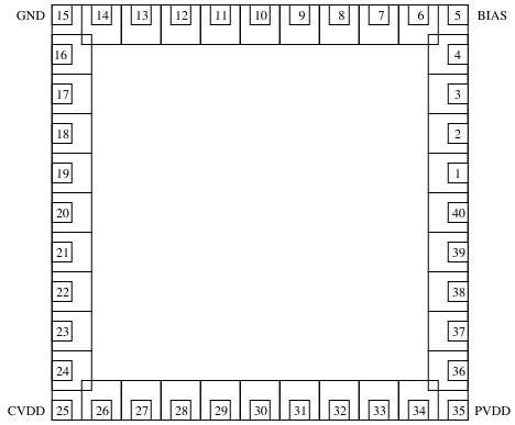
Figure 1. The pad frame showing the pin numbers and the locations of the "reserved" pads.
Figure 1 gives an overall picture of how the pad frame is arranged and the number of the pin to which each bonding pad will be connected when the chip is packaged (see Figure 2). There are a total of 40 pads with a usable core chip area of 3974λ × 3974λ (i.e., 1191 μm × 1191 μm). The four corner pads (i.e., those numbered 5, 15, 25, and 35) are "reserved." Pin 5 is a Bias voltage pin would be used to bias "analog" pads (e.g., an output buffer), if any existed in the pad set. It has the same basic protection structure as the inpad. Bias is routed into the core all around the pad frame and you may use it as a bias voltage connected to gates. There is some on-chip decoupling capacitance on the Bias line, so you should NOT use it for signals you expect to be able to change quickly. Pin 15 is ground (Gnd). Pin 25 is Vdd for the core of the chip, Pin 35 is Vdd for the pad frame. Ground and core Vdd (CVdd) are available all around the pad frame in either metal1 or metal2. You are free specify the type of pad that will go into each of the nine locations along the top, bottom, left, and right of the pad frame.
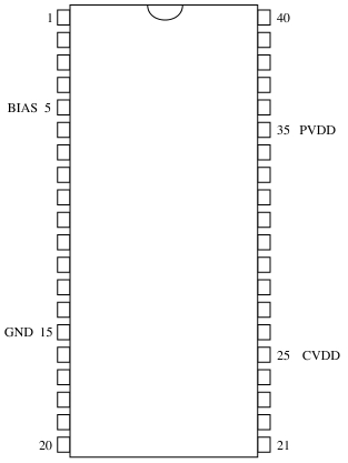
Figure 2. Top view of the 40-pin dual in-line package (DIP) in which your chip will packaged and returned.
To put your project in a pad frame, obtain the zip archive containing the pads and the pad frame cells in a Glade library and unzip it into your project directory. The top-level cell containing the pad frame is called "chip." Initially, all of the pads along the top, bottom, left, and right are blankpads. Copy all of the cells in the padframe library into your project library. Open the "chip" cell and instance the top-level cell for your design somewhere inside the pad frame in the chip cell.
To change a particular pad instance from a blankpad to another type of pad select the pad instance and hit the 'q' hotkey (or select Edit > Query) to bring up the Query dialog. In the 'Inst' tab, change the 'Cell Name' field from 'blankpad' to the name of whichever pad you want and hit return.
Once you have specified each of the pads, you should then route core Vdd, ground, and all of your I/O signals from the pad frame to the core (or vice versa) using either rectanlges or paths. Of course, you can also place the pads and do the routing incrementally, whichever is more convenient for you. Once you have finished making all of the connections between the core and the pads, you should extract the entire chip and select each pad net in the extracted view of the cell and verify that only those areas of the chip that should be connected to that pad are selected. You should be able to catch many kinds of shorts and forgotten connections in this way.