|
|
Mixed Analog-Digital VLSI I |
![]()
The blankpad is just a bonding pad with no connection to the core of the chip. It exists simply to fill empty space and complete the bias rings around the pad frame. All of the non-corner pads are initially blankpads.

The barepad is a bonding pad with a metal wire to the core of the chip. This pad has NO ESD PROTECTION, and so should be used with caution, and then only for nodes connected to a lot of source/drain regions. This pad is useful for providing additional power and ground pins (or some other supply voltage) and for measuring small currents without having any leakage from protection structures. This one is DEFINITELY NOT for inputs tied exclusively to gates!
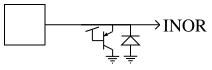
The inorpad is a bonding pad with a metal wire to the core of the chip and with "clamping" ESD protection. There is a reversed biased diode to the substrate, which will prevent the input from going more than one diode-drop below ground. There is a vertical PNP whose emitter is connected to the input, whose collector is the substrate, and whose base is connected to pad Vdd. The bipolar prevents the input from going more than one diode-drop above pad Vdd. This pad is suitable for connecting to source/drains. It's probably not a good idea to use this for inputs connected exclusively to gates.
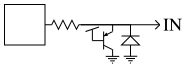
The inpad is an inorpad with a series poly resistor between the bonding pad and the clamping circuitry. There is a reversed biased diode to the substrate, which will prevent the input from going more than one diode-drop below ground. The diode and PNP prevent the end of the resistor nearest the core of the chip from going more than a diod-drop outside of the power supply. The resistor allows a voltage drop between the bonding pad and the clamping circuitry. This pad is suitable protection for gates. Please note that no ESD protection circuitry is a substitute for careful chip handling practices.
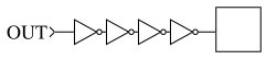
The outpad is a digital output pad. It comprises a cascade of four progressively sized inverters. The first inverter is sized so as to not present too large of a capacitive load for small gates to drive while the output inverter is sized to drive off-chip loads quickly.